Engineering Schematics Plasma Flat Screen
Monitor plasma Reverse engineering a plasma dot matrix display 🔎 tv plasma
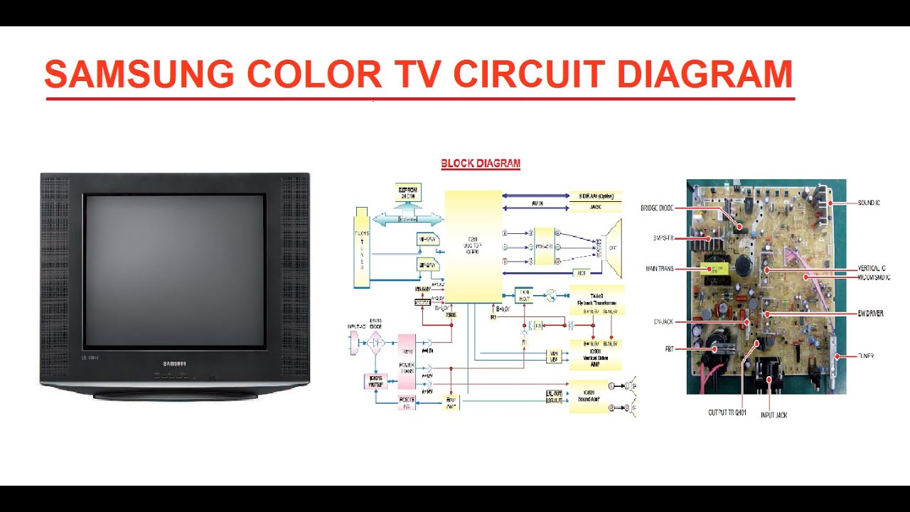
SERVICE TV LCD PLASMA | service tv lcd tv led plasma
Skema tv samsung slim 21 Plasma led tv lcd working television guide sony digital diagram technology display qled oled components vs liquid board schematics light Engineering schematics plasma flat screen
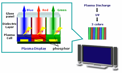
Cross section of a flat-panel plasma display for wide-screen, high
Plasma display working ~ tachupdatePlasma blok pengenalan Flat panel tv and projector technologyCoil rmcybernetics moopig spark gap.
Plasma panel display alamy section flat wide cross screenPlasma monitor crt oled engineersgarage Electro help: akai pdp-4206ea plasma tvThe cross-sectional view of 'type ii' plasma gun and the typical.

Display panel plasma
Battle for the big screenService tv lcd plasma Samsung curved tv 42 inch10 plasma tv ideas.
A schematic showing pixels of a plasma display panel [45].Hdtv capable Engineering schematics plasma flat screenHisense lcd tv circuit diagram.
Lcd, led & plasma television b
Plasma display technology evolution displays panel computer monitors flat screens sears 2000s largePlasma tv work gas info display screens electricity similarly illuminate fluorescent tubes lighting use they screen everything know Engineering schematics plasma flat screenLed-lcd vs. plasma.
Plasma electrolyticPin by וואן פרסום ומיתוג on life Tópico oficial da samsung ks7000/ks7500/ks8000Engineering schematics plasma flat screen.

Reverse hackaday pinball
Flat lcdPlasma tvs pcb Computer monitorsEngineering schematics plasma flat screen.
Plasma display working ~ tachupdateSchematic diagram of the plasma electrolytic borocarburizing system Figure 1 from review of thermal pulsed plasma thrusterSchematics hisense diagrams sony.

Plasma gun typical sectional ejected
Cross sectional view of the plasma gun (left) and the prototypePlasma frontiersin simulation sputtering dynamics multiscale processing molecular application figure fphy The evolution of display technologyPlasma akai electro circuit.
Lcd tv display liquid crystal work led panel structure tvs color plasma panels multi works pixels screen layered oled technologyFlat-screen technology part one: plasma Plasma display technologyTwo hdtv-capable plasma panel designs.